16.2 SYNCHRONOUS PIPELINING AND CLOCKING STYLES
Consider a typical synchronous nonpipelined system as shown in Fig. 16.1(a). Here, the system consists of a single combinatorial block surrounded by edge triggered registers. At the beginning of each clock cycle, data is initiated into the block from the input register. Due to the differences in circuit path lengths and other factors, the delay through the combinatorial block may vary. However, this delay is bounded between tmin and tmax as shown in Fig. 16.1(b). Here, the shaded regions depict the flow of data through the combinatorial block and the times at which particular parts of the logic are changing, while the unshaded regions depict the time at which the logic is stationary. Therefore, the output register is clocked in the unshaded region after the latest data has arrived at the output of the combinatorial block (allowing for register setup times). At the same time new input data is clocked into the logic at the input register. Therefore, the minimum clock period is bounded by the sum of the longest delay of the combinatorial logic and the propagation, setup times of the register together with any unintentional clock skew between input and output clocks.
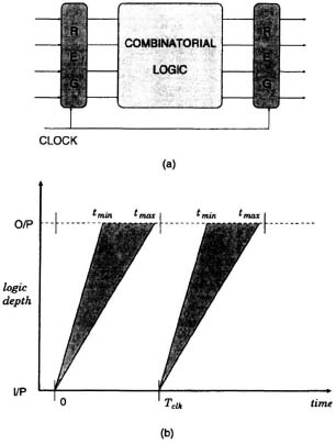
Fig. 16.1 (a) Synchronous nonpipelined system. (b) Data flow.
The conventional method for decreasing the clock period of the system is by pipelining the combinatorial ...
Get VLSI Digital Signal Processing Systems: Design and Implementation now with the O’Reilly learning platform.
O’Reilly members experience books, live events, courses curated by job role, and more from O’Reilly and nearly 200 top publishers.

