13.3 Substrate Growth and Preparation
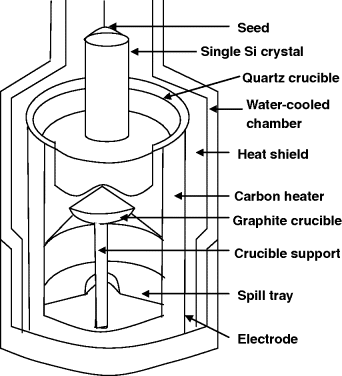
The typical semiconducting substrate material is either silicon or compound semiconductors like GaAs or InP. These are crystalline materials in the form of large cylindrical ingots grown through a phase change from one of the three phases (vapor, liquid or amorphous solid) into a crystalline solid phase. The liquid-to-crystalline solid-phase transition is the most common method. In this case, a small seed crystal of the material to be grown is allowed to touch the surface of the melt of the material and is pulled slowly out of the melt, as a result of which each successive plane of atoms attaches to the surface of the seed crystal in the correct relative position and orientation. We illustrate this method of growth by the diagram shown in Figure 13.1, in which a Si single crystal is grown by the Czochralsky method.
Figure 13.1 The Czochralsky method of growing single-crystal silicon.
In the Czochralsky method, the silicon boule is reshaped after recovery from the crystal puller. The ends are removed by sawing together with flawed regions, and the remainder is put to the shape of a cylindrical ingot on a lathe. By using X-ray diffraction, the crystal axes are identified and orientational flats are ground on the surface so as to identify the axes at later times. The boule is then sawed into thin wafers by using diamond-impregnated saw blades. ...
Get Silicon Photonics: Fundamentals and Devices now with the O’Reilly learning platform.
O’Reilly members experience books, live events, courses curated by job role, and more from O’Reilly and nearly 200 top publishers.

