4.4 Absorption Processes in Semiconductors
The absorption process in semiconductors can best be understood with the help of quantum mechanical theory. The radiation then is assumed to be a bunch of photons. When incident on a semiconductor, this bunch induces transitions among different energy levels in different bands in the material. A few representative transitions occurring in a semiconductor are illustrated in Figure 4.2 by using the E–k diagram.
Figure 4.2 Illustration of the different absorption processes in semiconductors.
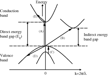
The process indicated by (A) in Figure 4.2 represents direct valence to conduction band transitions (constant k vector) that occurs in a direct band gap semiconductor, like GaAs. Process (B) illustrates indirect valence to conduction band transitions aided by photon–phonon coupling interactions. Process (C) represents intervalence band transitions, for example, transition between heavy-hole (HH) and split-off (SO) bands. Process (D) depicts valence band free-carrier transitions aided by impurities or photon–phonon interactions. Process (E) is for free-carrier transitions in conduction band aided by impurities or photon–phonon interactions. Depending on the photon energy, a single type or a combination of a few types of all the absorption processes indicated in the figure may be important. We shall discuss the origin and characteristics of these processes ...
Get Silicon Photonics: Fundamentals and Devices now with the O’Reilly learning platform.
O’Reilly members experience books, live events, courses curated by job role, and more from O’Reilly and nearly 200 top publishers.

