5.2 SEQUENTIAL CIRCUITS
5.2.1 Decade Counter
This design was implemented for a Xilinx 3020 FPGA with the aid of the ViewDraw schematic entry program, the ViewSim simulator, and Xilinx software for CLB mapping, placement, routing, and so on. The design illustrates alternative ways of creating a decade counter:
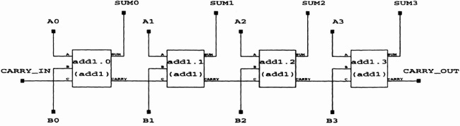
Figure 5–7. Schematic for ripple adder.
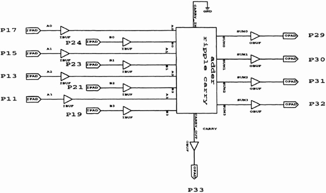
Figure 5–8. Top-level schematic for ripple adder.
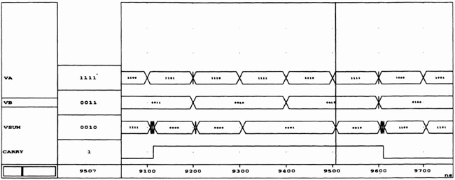
Figure 5–9. Simulation for ripple adder.
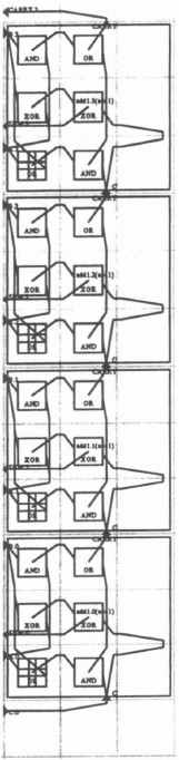
Figure 5–10. CAL layout for ripple adder.
- Using a macro element for a synchronous decade counter functionally equivalent to the 74160 TTL component
- As a collection of gates and flip-flops
- By direct entry to CLBs
Figure 5–11 shows the top-level schematic. The demonstration board has an RC controlled oscillator based on a single configurable logic block. The GOSC macro, shown in the lower left of the figure, produces a clock that runs at approximately 100 Hz when connected to external R and C components through pins 12 and 14. Another pin is connected to a dual in-line package switch that determines if counting takes place, or otherwise holds the ...
Get Field-Programmable Gate Arrays: Reconfigurable Logic for Rapid Prototyping and Implementation of Digital Systems now with the O’Reilly learning platform.
O’Reilly members experience books, live events, courses curated by job role, and more from O’Reilly and nearly 200 top publishers.

