Example 4. High-speed Digital Design
This example demonstrates how to stack up layers and design transmission lines for a high-speed digital PCB. The example also demonstrates how to create a moated ground area with a bridge around a high-frequency crystal oscillator, how to perform pin/gate swapping, and how to create a heat spreader using vias to the Ground plane. The example circuit is shown in
Figure 9-156
.
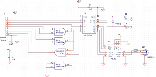 |
| Figure 9-156 High-speed digital circuit schematic. |
The BOM for this example is shown in
Table 9-8 . The circuit consists of a (fictional) high-speed, low-pin-count microcontroller/digital signal processor (uP-EXD10) driven by a 66-MHz clock ...
Get Complete PCB Design Using OrCAD Capture and PCB Editor now with the O’Reilly learning platform.
O’Reilly members experience books, live events, courses curated by job role, and more from O’Reilly and nearly 200 top publishers.

