16.12 PROBLEMS
- Consider a typical sequential system shown in Fig. 16.59 which is designed using CLBs and latches (LATs). Let us assume that the input signal to the leftmost latch is [Vϕ1] and that the latch is clocked using ϕ1. Will this sequential circuit behave correctly? Explain. Also, what is the status of the signals at nodes 1–8, i.e., are they [Vϕ1], [Vϕ2], [Sϕ1], or [Sϕ2]? Explain which latches are clocked using ϕ1 and which are clocked using ϕ2.
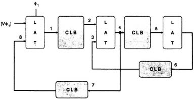
Fig. 16.59 A typical sequential system.
- Consider the circuit shown in Fig. 16.60, where the input signal X is [Vϕ1] and the input signal Y is [Sϕ1]. The signal Z is used as the clock for the latch. Will this latch function correctly? If so, what is the main advantage of this circuit?
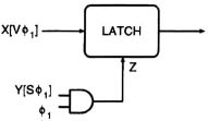
Fig. 16.60 Circuit for Problem 2.
- Draw the timing waveforms of ϕ, ϕ1, and ϕ2 for the circuit shown in Fig. 16.8 and verify the operation of the 2-phase clock generator.
- Design a 9-transistor positive edge-triggered true single phase clocked flip-flop and explain its operation.
- Let us assume that a bit-pipelined digital system is designed using a single-phase level sensitive clocking scheme with pulse width tϕ. Show that the clock skew δ for this clocking scheme is given by
Explain the behavior of the circuit for both positive and negative ...
Get VLSI Digital Signal Processing Systems: Design and Implementation now with the O’Reilly learning platform.
O’Reilly members experience books, live events, courses curated by job role, and more from O’Reilly and nearly 200 top publishers.

