23D Memory Using Double-Gate, Folded, TFT, and Stacked Crystal Silicon
2.1 Introduction
An early step in moving from a planar memory technology to a vertical technology has been moving from a planar gate to a vertical gate device such as the fin-shaped field-effect transistor (FinFET) flash memory or other folded vertical memory structure. In the case of the FinFET, the short-channel effect, which is a limitation on the channel length created by scaling, is eliminated. The vertical FinFET also offers the potential for a double or triple gate, which enhances transistor and memory 3D characteristics.
An illustration of a FinFET transistor structure is shown in Figure 2.1. The vertical silicon fin forms the channel in which the current flows laterally. The transistor gate oxide and the polysilicon gate are patterned on the fin. The channel length is determined by the thickness of the gate, and the channel width is determined by the height of the fin. This structure permits increased channel length, which improves gate control, eliminating short-channel effects, and increases ON current by permitting increased channel width. It also provides a double gate with one gate on each side of the fin, which enhances gate control.
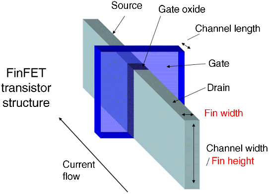
Figure 2.1 Schematic of a 3D FinFET transistor structure.
Thin-film transistors (TFTs) are also discussed in this chapter. TFTs can be used to form 3D vertical ...
Get Vertical 3D Memory Technologies now with the O’Reilly learning platform.
O’Reilly members experience books, live events, courses curated by job role, and more from O’Reilly and nearly 200 top publishers.

