2.2 PIC18F2410 Architecture
The pin configuration (DIP package) of the PIC18F2410 microcontroller is shown in Figure 2.2. As we shall see later, most of the pins are multiplexed and can be used for different purposes. For example, pin 2 is named as RA0/AN0 and this is the PORT A least significant port pin. This pin can be used as an analogue input (named AN0), or as a digital I/O (named RA0).
Figure 2.2 PIC18F2410 pin configuration (DIP package). (Reproduced with permission from Microchip Inc)
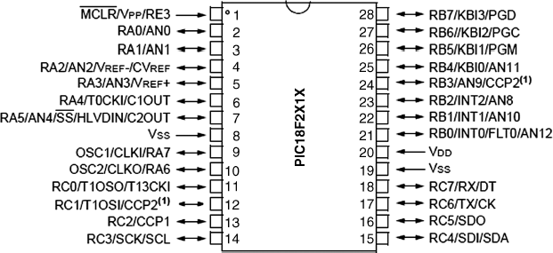
Figure 2.3 shows the simplified internal architecture of the PIC18F2410 microcontroller. The CPU is at the centre of the diagram and consists of an 8-bit ALU, an accumulator register (WREG), and an 8 × 8 multiplier module. The multiplier takes data from the accumulator register and the data bus, and provides the 16-bit result in registers PRODH and PRODL, where the result can be read through the data bus.
Figure 2.3 Internal architecture of the PIC18F2410 microcontroller. (Reproduced with permission from Microchip Inc)
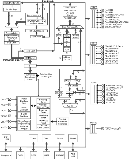
The program memory and the program counter are shown at the top left corner of the figure. The memory address consists of 21 bits, capable of addressing up to 2 MB of memory data, although here only 16 KB is used. The program counter consists of two 8-bit registers PCH and ...
Get Using LEDs, LCDs and GLCDs in Microcontroller Projects now with the O’Reilly learning platform.
O’Reilly members experience books, live events, courses curated by job role, and more from O’Reilly and nearly 200 top publishers.

