ANSWERS TO PROBLEMS
CHAPTER 1
1.1 R1 = 2941 Ω, R2 = 1515 Ω
1.2 R1 = 930 Ω, R2 = 1400 Ω
1.3 R1 = 85.24 kΩ, R2 = 41.84 kΩ, R3 = 23.43 kΩ
1.4 For a current source, the current will remain constant regardless of the voltage so Z = dV/di = ∞. The DC current source should be represented as an open circuit.
1.5 874.8 Ω
1.6 (a) Attenuation: VO/VIN, 1/3
(b) DC bias, 2.5 V
(c) Load impedance, 27 kΩ
(d) Source impedance, 6 kΩ
1.7 115 mA
1.8 624 mW
CHAPTER 2
2.1 PD = 16 W
2.2 TJ = 196°C
2.3 The junction temperature would rise to 193°C which would compromise the MTBF of the transistor.
2.4 The thermal resistance must be less than 5.87 °C/W so about 130 FPM is required.
2.5 2 J/°C
CHAPTER 3
3.1 Transfer functions for a through d are
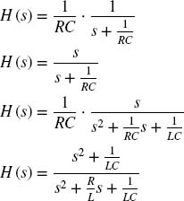
3.2 The transfer function is
![]()
where
and
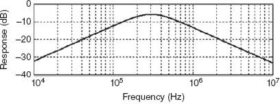
The frequency response is
Frequency response plot for Problem 3.2.
3.3 The updated network is
Updated network for Problem 3.3.
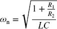
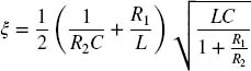
3.4 The transfer function is
where the networks from left to right are A, B, and C.
The ...
Get Ten Essential Skills for Electrical Engineers now with the O’Reilly learning platform.
O’Reilly members experience books, live events, courses curated by job role, and more from O’Reilly and nearly 200 top publishers.

