8.5 Examples of Photodiodes in Standard Silicon Technology
We begin by illustrating the richness in possibilities for the types of photodiodes that can be made with standard or mainstream CMOS technology. In particular, we discuss several possibilities in a standard 0.18 µm CMOS technology as illustrations of what may be possible. Typically, this technology offers many layers such as n+, p+, n-well, p-well, and p-substrate that could be suitably combined to make photodiodes. Figure 8.10 illustrates several of these photodiode options.
Figure 8.10 Some of the possibilities of photodiodes in standard CMOS technology. Note the differences in doping concentrations as well as junction depths which would contribute to varying optimum wavelength responses and quantum efficiencies.
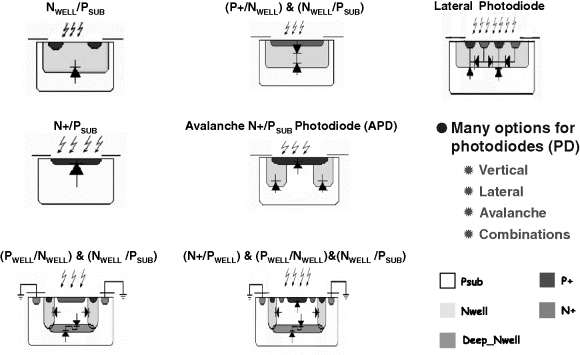
In general, the responsivity of these diodes varies because the depletion regions of the junctions are at different distances from the surface of the silicon substrate and the doping concentrations are different. Deeper junctions are more responsive to longer wavelengths of incident radiation. Also, to a first order, the responsivity depends on the volume of the depletion region which also depends on the doping concentrations and doping profiles. The photocurrent IPC in a junction photodiode can be written as
In Eq. (8.27), GOP is the generation rate of electron–hole pairs from the absorbed light,
Get Silicon Photonics: Fundamentals and Devices now with the O’Reilly learning platform.
O’Reilly members experience books, live events, courses curated by job role, and more from O’Reilly and nearly 200 top publishers.

