1.3 The Interconnect Problem in VLSI
On-chip interconnect is nothing but electrical wiring. According to the International Technology Roadmap for Semiconductors (ITRS), an interconnect is electrical wiring that distributes clock and other signals, and provides power and ground to and among the various circuits or systems functions on a chip.
The process devoted to metallization and interconnect involves deposition of metals, interlevel dielectrics deposition, and etching steps. A typical interconnect structure is shown in Figure 1.2.
Figure 1.2 Schematic view of electrical interconnect in very large-scale integrated (VLSI) circuit.
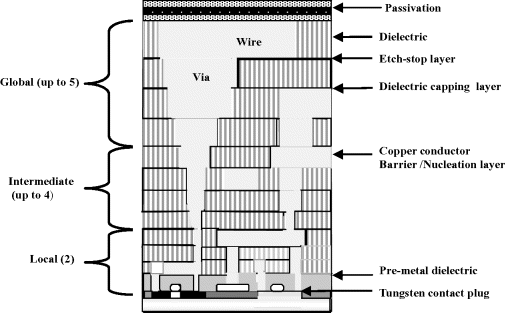
The earlier approach was aluminum deposition and dry-etch definition. Currently, copper wires are introduced. The global wires connect different functional units, distributing clock signals and power among them. The length of the global wires scales down with chip size. On the other hand, local wires connect the gates, sources, and drains of close MOSFETs of the same functional units and their length scales with gate size.
Although the downscaling of transistor increases the speed, the same is not true for the downsizing of interconnect. In earlier ICs in use around the 1980s, the delay in interconnects was propagation limited, that is, it was limited by the time of propagation of the electromagnetic waves associated to SiO2, rather than the RC time ...
Get Silicon Photonics: Fundamentals and Devices now with the O’Reilly learning platform.
O’Reilly members experience books, live events, courses curated by job role, and more from O’Reilly and nearly 200 top publishers.

