From pin configuration registers, to debouncing buttons, to timers, this chapter will describe the most basic embedded concepts, focusing on the input and output aspects of the system. To keep it interesting, weâll work through an example product, going through the phases of a project as the vision appears, changes, and finally crystallizes. Even the simple-sounding subject of making an LED blink is not immune to changes in product goals.
Marketing has come to you with an idea for a product. When you see through the smoke and mirrors, you realize that all they need is a light to blink.
Most processors have pins whose digital states can be read (input) or set (output) by the software. These go by the name of I/O pins, general-purpose I/O (GPIO), and occasionally general I/O (GIO). The basic use case is usually straightforward, at least when an LED is attached:
Initialize the pin to be an output (as an I/O pin, it could be input or output).
Set the pin high when you want the LED on. Set the pin low when you want the LED off. (Although the LED also can be connected to be on when the pin is low, but this example will focus on noninverted logic.)
Through this chapter, Iâll give you examples from three different user manuals so you get an idea of what to expect in your processorâs documentation. Atmelâs ATtiny AVR microcontroller manual describes an 8-bit microcontroller with plenty of peripherals. The TI MSP430x2xx Userâs Guide describes a 16-bit RISC processor designed to be ultra low power. The NXP LPC13xx User Manual describes a 32-bit ARM Cortex microcontroller. You wonât need these documents to follow along, but I thought you might like to know the processors the examples are based upon.
To do anything with an I/O line, we need to talk to the appropriate register. As described in Reading a Datasheet, you can think of registers as an API to the hardware. Described in the chipâs user manual, registers come in all flavors to configure the processor and control peripherals. They are memory-mapped, so you can write to a specific address to modify a particular register.
As you work with registers, you will need to think about things at
the bit level. Often youâll turn specific bits on and off. If youâve
never used bitwise operations, now is the time to look them up. In C and
C++, a bitwise-OR is | and bitwise-AND is
&. The logical NOT operator
(!) turns a 1 into a 0 (or a true into a false), and
vice versa. The bitwise NOT (~) sets each bit to its
opposite value:
register = register | (1 << 3); // turn on the 3rd bit in the register
register |= 1 << 3;             // same, but more concisely
register &= ~(1 << 3);          // turn off the 3rd bit in the register
Enough review. If this isnât pretty obvious, look into bitwise operations and Boolean math. You will need to know these pretty well to use registers.
Most I/O pins can be either inputs or outputs. The first register youâll need to set will control the direction of the pin so it is an output. First, determine which pin you will be changing. To modify the pin, youâll need to know the pin name (âI/O pin 2,â not its number on the processor (for example, pin 12). The names are often inside the processor in schematics where the pin number is on the outside of the box (as shown in Figure 4-1).
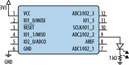
The pins may have multiple numbers in their name, indicating a port (or bank) and a pin in that port. (The ports may also be letters instead of numbers.) In the figure, the LED is attached to processor pin 10, which says âSCLK/IO1_2.â This pin is shared between the SPI port (remember, this is a communication method, discussed in Chapter 6) and the I/O subsystem (IO1_2). The user manual will tell you whether the pin is an I/O by default or a SPI pin (and how to switch between them). Another register may be needed to indicate the purpose of the pin. Most vendors are good about cross-referencing the pin setup, but if it is shared between peripherals, you may need to look in the peripheral section to turn off unwanted functionality. In our example, weâll say the pin is an I/O by default.
In the I/O subsystem, it is the second pin (2) of the first bank (1). Weâll need to remember that and to make sure the pin is used as an I/O pin and not as a SPI pin. Your processor user manual will describe more. Look for a section with a name like âI/O Configuration,â âDigital I/O Introduction,â or âI/O Ports.â If you have trouble finding the name, look for the word âdirection,â which tends to be used to describe whether you want the pin to be an input or an output.
Once you find the register in the manual, you can determine whether you need to set or clear a bit in the direction register. In most cases, you need to set the bit to make the pin an output. You could determine the address and hardcode the result:
*((int*)0x0070C1) |= (1 << 2);
However, please donât do that.
The processor or compiler vendor will almost always provide a header that hides the memory map of the chip so you can treat registers as global variables. If they didnât give you a header, make one for yourself so that your code looks more like one of these lines:
Note that the register names are different for each processor, but the effect of the code in each line is the same. Each processor has different options for setting the second bit in the byte (or word).
In each of these examples, the code is reading the current register value, modifying it, and then writing the result back to the register. This read-modify-write cycle needs to happen in atomic chunks. If you read the value, modify it, and then do some other stuff before writing the register, you run the risk that the register has changed and the value you are writing is out of date. The register modification will change the intended bit, but also might have unintended consequences.
The next step is to turn on the LED. Again, weâll need to find the appropriate register in the user manual.
The header file provided by the processor or compiler vendor shows how the raw addresses get masked by some programming niceties. In the LPC13xx.h, the I/O registers are accessed at an address through a structure (I made some reorganization and simplifications to the file):
typedef struct{
  __IO uint32_t DATA;
  uint32_t RESERVED0[4095]; // The same data appears at 4096 locations
                            // in the GPIO address space, and 12 bits
                            // of the address bus can be used for
                            // bit masking. (See manual 7-4.1)

  __IO uint32_t DIR;  // direction set for output, clear for input
  __IO uint32_t IS;   // interrupt sense (1 = interrupt pending)
  __IO uint32_t IBE;  // interrupt on both falling and rising edges
  __IO uint32_t IEV;  // interrupt event register
  __IO uint32_t IE;   // interrupt enable
  __IO uint32_t RIS;  // raw status register
  __IO uint32_t MIS;  // masked interrupt status register
  __IO uint32_t IC;   // interrupt clear (set bit to clear interrupt)
} LPC_GPIO_TypeDef;

#define LPC_AHB_BASE          (0x50000000UL)
#define LPC_GPIO0_BASE        (LPC_AHB_BASE  + 0x00000)
#define LPC_GPIO1             ((LPC_GPIO_TypeDef   *) LPC_GPIO1_BASE )
The header file describes many registers we havenât looked at. These are also in the user manual section, with a lot more explanation. I prefer accessing the registers via the structure because it groups related functions together, often letting you work with the ports interchangeably.
Tip
You may want to update a vendor header file to use this structured approach. Approach this free code as a starting point, not the final draft. Modify it as needed to work in your system.
Once we have the LED on, weâll need to turn it off again. You just need to clear those same bits, as shown in the register section (Starting with Registers):
To finish our program, all we need to do is put it all together. The pseudocode for this is:
main:
  initialize the direction of the I/O pin to be an output
loop:
  set the LED on
  do nothing for some period of time
  set the LED off
  do nothing for the same period of time
  repeat
Once youâve programmed it for your processor, you should compile, load, and test it. You might want to tweak the delay loop so the LED looks about right. It will probably require several tens of thousands of processor cycles, or the LED will blink faster than you can perceive it.
If you have a debugging system such as JTAG set up, finding out why your LED wonât turn on is likely to be straightforward. Otherwise, you may have to use the process of elimination.
First, check to see whether a pin is shared between different peripherals. While we said that the pin was an I/O by default, if you are having trouble, verify that its functionality is as expected.
As long as you have the manual open, verify that the pin is configured properly. If the LED isnât responding, youâll need to read the peripherals chapter of the user manual. Processors are different, so check that the pin doesnât need additional configuration (e.g., a power control output) or have a feature turned on by default (do not make the GPIO an open-drain output by accident).
Most processors have I/O as a default because that is the simplest way for their users (us!) to verify the processor is connected correctly. However, particularly with low-power processors, they want to keep all unused subsystems off to avoid power consumption. (And other special-purpose processors may have other default functionality.) The user manual will tell you more about the default configuration and how to change it. These are often other registers that need a bit set (or cleared) to make a pin act as an I/O.
Next, make sure the system is running your code. Do you have another way to verify that the code being run is the code that you compiled? If you have a debug serial port, try incrementing the revision to verify that the code is getting loaded.
Make the code as simple as possible to be certain that the processor is running the function handling the LEDs. Eliminate any noncritical initialization of peripherals in case the system is being delayed while waiting for a nonexistent external device. Turn off interrupts and asserts. Make sure the watchdog is off (see Watchdog). Put the LED code in the larger piece of code as early as possible, to reduce the likelihood that any other code is freezing the processor.
Double-check your math. Even if you are completely comfortable with hex and bit shifting, a typo is always possible. In my experience, typos are the most difficult bugs to catch, often harder than memory corruptions. Check you are using the correct pin on the schematic. And make sure there is power to the board. (You may think that advice is funny, but youâd be surprised at how often this plays a role!)
With many microcontrollers, pins can sink more current than they can source (provide). Therefore, it is not uncommon for the pin to be connected to the cathode rather than the anode of the LED. In these instances, you turn on an LED by writing a zero rather than a one.
If the output still doesnât work, consider whether there is a hardware issue. Even in hardware, it can be something simple (installing LEDs backward is pretty easy). It may be a design problem such as the processor pin being unable to provide enough current to drive the LED; the datasheet (or user manual) might be able to tell you this. There might be a problem on the board, such as a broken component or connection. With the high-density pins on most processors, it is very easy to short pins together. Ask for help, or get out your multimeter (or oscilloscope).
Marketing liked your first prototype, though they might want to tweak it a bit later. The system went from a prototype board to a PCB. During this process, somehow the pin number changed (to IO1_3). They need to be able to run both systems.
It is trivially simple to fix the code for this project, but for a larger system, the pins may be scrambled to make way for a new feature. Letâs look at how to make modifications simpler.
Using a board-specific header file lets you avoid hardcoding the pin. If you have a header file, you just have to change a value there instead of going through your code to change it everywhere itâs referenced. The header file might look like this:
#define LED_SET_DIRECTION  (P1DIR)
#define LED_REGISTER       (P1OUT)
#define LED_BIT            (1 << 3)
The lines of code to configure and blink the LED can be processor-independent:
LED_SET_DIRECTION |= LED_BIT; // set the I/O to be output
LED_REGISTER |= LED_BIT;      // turn the LED on
LED_REGISTER &= ~LED_BIT;     // turn the LED off
That could get a bit unwieldy if you have many I/O lines or need the other registers. It might be nice to be able to give only the port (1) and position in the port (3) and let the code figure it out. The code might be more complex, but it is likely to save time (and bugs). For that, the header file would look like this:
// ioMapping_v2.h
#define LED_PORT 1
#define LED_PIN 3
If we want to recompile to use different builds for different boards, we can use three header files. The first is the old board pin assignments (ioMapping_v1.h). Next, weâll create one for the new pin assignment (ioMapping_v2.h). We could include the one we need in our main .c file, but that defeats the goal of modifying that code less. If we have the main file always include a generic ioMapping.h, we can switch the versions in the main file by including the correct header file:
// ioMapping.h
#if COMPILING_FOR_V1
#include "ioMapping_v1.h"
#elif COMPILING_FOR_V2
#include "ioMapping_v2.h"
#else
#error "No I/O map selected for the board. What is your target?"
#endif /* COMPILING_FOR_*/
Using a board-specific header file hardens your development process against future hardware changes. By sequestering the board-specific information from the functionality of the system, you are creating a more loosely coupled and flexible code base.
Tip
Keeping the I/O map in Excel is a pretty common way to make sure the hardware and software engineers agree on the pin definitions. With a little bit of creative scripting, you can generate your version-specific I/O map from a CSV file to ensure your pin identifiers match those on the schematic.
Instead of writing directly to the registers in the code, weâll need to handle the multiple ports in a generic way. So far we need to initialize the pin to be an output, set the pin high so the LED is on, and set the pin low so the LED is off. Oddly enough, we have a large number of options for putting this together, even for so simple an interface.
In the implementation, the initialization function configures the pin to be an output (and sets it to be an I/O pin instead of a peripheral if necessary). With multiple pins, you might be inclined to group all of the initialization together, but that breaks the modularity of the systems.
Although the code will take up a bit more space, it is better to have each subsystem initialize the I/Os it needs. Then if you remove or reuse a module, you have everything you need in one area. However, weâve seen one situation where you should not separate interfaces into subsystems: the I/O mapping header file, where all of the pins are collected together to make the interface with the hardware more easily communicated.
Moving on with the I/O subsystem interface, setting a pin high and
low could be done with one function: IOWrite(port, pin, high/low). Alternatively,
this could be broken out so that there are two functions: IOSet(port, pin) and IOClear(port, pin). Both methods work. Imagine
what our main function will look like in both cases.
The goal is to make the LED toggle. If we use IOWrite, we can have a variable that switches
between high and low. In the IOSet
and IOClear case, weâd have to save
that variable and check it in the main loop to determine which function
to call. Alternatively, we could hide IOSet and IOClear within another function called
IOToggle.
XOR
XOR (exclusive or) is a somewhat magical bitwise operation. It doesnât have a logical analog and isnât used as much as the others weâve seen, so remembering it can be tough.
Imagine your nemesis puts on his blog that he is going to the movies this evening, which is just what you had planned to do. If you both avoid going, the movie wonât play, because there wonât be an audience. One of you can go to see the movie. But if you both go, the movie wonât play (the theater is still not happy about the fuss you caused last time).
The truth table looks like:
| Input A | Input B | Output |
|---|---|---|
| 0 | 0 | 0 |
| 0 | 1 | 1 |
| 1 | 0 | 1 |
| 1 | 1 | 0 |
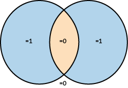
XOR is often represented as a Venn diagram, as shown in Figure 4-2. Note that XOR is true inside each circle, but not where they overlap.
XOR has some nifty applications in computer graphics and finding overflows (math errors). You can also toggle our LED on and off using XOR:
register = register ^ (1 << 2);
Note that (1 << 2) would always be a 1 in the table. If it is Input A, we are using only the bottom half of the chart. If the register (Input B) already has that pin set, what would the output be?
We donât have any particular constraints with our hardware, so we donât need to consider optimizing the code in this example. For educationâs sake, however, consider the options we are giving ourselves with these potential interfaces.
The IOWrite option does
everything in one function, so it takes less code space. However, it has
more parameters, so it takes more stack space, which comes out of RAM.
Plus it has to keep around a state variable (also RAM).
With the IOSet/IOClear/IOToggle option, there are more functions
(more code space), but fewer parameters and possibly no required
variables (less RAM). Note that the toggle function is no more expensive
in terms of processor cycles than the set and clear functions.
This sort of evaluation requires you to think about the interface along another dimension. Chapter 8 will go over more details on how to optimize for each area. During the prototyping phase, it is too soon to optimize the code, but it is never too soon to consider how the code can be designed to allow for optimization later.
The modifications in the previous sections put the I/O-handling code in its own module, though the basics of the main loop donât change. The implementation might look like the following:
void main(void){
IOSetDir(LED_PORT, LED_PIN, OUTPUT);
while (1) { // spin forever
IOToggle(LED_PORT, LED_PIN);
DelayMs(DELAY_TIME);
}
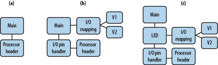
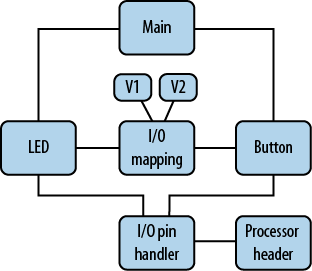
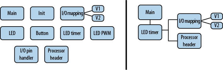
}The main function is no longer directly dependent on the processor. With this level of decoupling, the code is more likely to be reused in other projects. In (a) of Figure 4-3, the original version of software architecture is shown, with its only dependency being the processor header. The middle, labeled (b), is our current version. It is more complicated, but the separation of concerns is more apparent. Note that the header files are put off to the side to show that they feed into the dependencies.
Our next reorganization will create an even more flexible and reusable architecture, illustrated by (c).
As you can imagine, our I/O interface is going to get more complex as the product features expand. (Currently we have only one output pin, so it canât really get any simpler.) In the long run, we want to hide the details of each subsystem. There is a standard software design pattern called facade that provides a simplified interface to a piece of code. The goal of the facade pattern is to make a software library easier to use. Along the lines of the metaphor Iâve been using in this book, that interfacing to the processor is similar to working with a software library, it makes sense to use the facade pattern to hide some details of the processor and the hardware.
In the section From Diagram to Architecture, we saw the adapter pattern, which is a more general version of the facade pattern. Whereas the adapter pattern acted as a translation between two layers, the facade does this by simplifying the layer below it. If you were acting as an interpreter between scientists and aliens, you might be asked to translate âx=y+2, where y=1.â If you were an adapter pattern, youâd restate the same information without any changes. If you were a facade pattern, youâd probably say âx=3â because it is simpler and the details are not critical to using the information.
Hiding details in a subsystem is an important part of good design. It makes the code more readable and more easily tested. Furthermore, the calling code doesnât depend on the internals of the subsystem, so the underlying code can change, while leaving the facade intact.
A facade for our blinking LED would hide the idea of I/O pins from the calling code by creating an LED subsystem, as shown in the right side of Figure 4-3. Given how little the user needs to know about the LED subsystem, the facade could be implemented with only two functions:
LEDInit()Calls the I/O initialization function for the LED pin (replaces
IOSetDir(â¦))LEDBlink()Blinks the LED (replaces
IOToggle(â¦))
Adding a facade will often increase the size of your code, but may be worth it in terms of debuggability and maintainability.
Marketing has determined that they want to change the way the system blinks in response to a button. Now, when the button is held down, the system should stop blinking altogether.
Our schematic is not much more complex with the addition of a button (see Figure 4-4). Note that the button uses IO2_2 (I/O port 2, pin 2), which is denoted with S1 (switch 1). The icon for a switch makes some sense; when you push it in, it conducts across the area indicated. Here, when you press the switch, the pin will be connected to ground.
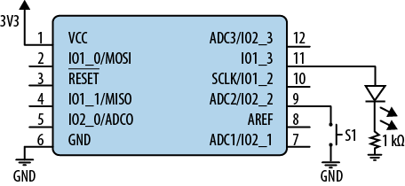
Many processor I/O pins have internal pull-up resistors. When a pin is an output, the pull-ups donât do anything. However, when the pin is an input, the pull-up gives it a consistent value (1), even when nothing is attached. The existence and strength of the pull-up may be settable, but this depends on your processor (and possibly on the particular pin). Some processors even have an option to allow internal pull-downs on a pin. In that case, our switch could have been connected to power instead of ground.
Tip
Inputs with internal pull-ups take a bit of power, so if your system needs to conserve a few microamps, you may end up disabling the unneeded pull-ups.
Your processor user manual will describe the pin options. The basic steps for setup are:
Add the pin to the I/O map header file.
Configure it to be an input. Verify that it is not part of another peripheral.
Configure a pull-up explicitly (if necessary).
Once you have your I/O pin set up as an input, youâll need to add a function to use it, one that can return the state of the pin as high (true) or low (false):
boolean IOGet(uint8_t port, uint8_t pin);
The button will connect to ground when the button is pressed. This signal is active low, meaning that when the button is actively being held down, the signal is low.
To keep the details of the system hidden, weâll want to make a button subsystem that can use our I/O-handling module. On top of the I/O function, we can put another facade so that the button subsystem will have a simple interface.
The I/O function returns the level of the pin. However, we want to know whether the user has taken an action. Instead of the button interface returning the level, you can invert the signal to determine whether the button is currently pressed. The interface could be:
void ButtonInit()Calls the I/O initialization function for the button
boolean
          ButtonPressed()
Returns true when the button is down
As shown in Figure 4-5, both the LED and button subsystems use the I/O subsystem and I/O map header file. This is a simple illustration of how the modularization we did earlier in the chapter allows reuse.
At a higher level, there are a few ways to implement the main function:
main:
  initialize LED
  initialize button
loop:
  if button pressed, turn LED off
  else toggle LED
  do nothing for a period of time
  repeat
With this code, the LED wonât go off immediately, but will wait until the delay has expired. The user may notice some lag between pushing the button and the LED turning off.
Tip
A system that doesnât respond to a button press in less than a quarter of a second (250 ms) feels sluggish and difficult to use. A response time of 100 ms is much better, but still noticeable to impatient people. A response time under 50 ms feels very snappy.
To decrease the response time, we could check constantly to see whether the button was pressed:
loop:
  if button pressed, turn LED off
  else
    if enough time has passed,
      toggle LED
      clear how much time has passed
  repeat
Both of these methods check the button to determine whether it is pressed. This continuous querying is called polling and is easy to follow in the code. However, if the LED needs to be turned off as fast as possible, you may want the button to interrupt the normal flow.
Wait! That word (interrupt) is a really important one. Iâm sure youâve heard it before, and weâll get into a lot more detail soon (and again in Chapter 5). Before that, look at how simple the main loop can be if you use an interrupt to capture and handle the button press:
loop:
  if button not pressed, toggle LED
  do nothing for a period of time
  repeat
The interrupt code (aka ISR, or interrupt service routine) would call the function to turn off the LED. However, this makes the button and LED subsystems depend on each other, coupling the systems together in an unobvious way. There are times where youâll have to do this so an embedded system can be fast enough to handle an event.
Chapter 5 will describe how and when to use interrupts in more detail. This chapter will continue to look at them at a high level only.
Instead of using the button to halt the LED, marketing wants to test different blink rates by tapping the button. For each button press, the system should decrease the amount of delay it has (until it gets to near zero, at which point it should go back to the initial delay).
In the previous assignment, all you had to check was whether the button was pressed down. This time you have to know both when the button will be pressed and when it will be released. Ideally, weâd like the switch to look like the top part of Figure 4-6. If it did, we could make the system note the rising edge of the signal and take an action there.
This might be another area where an interrupt can help us catch the user input so the main loop doesnât have to poll the I/O pin so quickly. The main loop becomes straightforward if it uses a global variable to learn about the button presses:
interrupt when the user presses the button:
  set global button pressed = true

loop:
  if global button pressed,
    set the delay period (reset or decrease it)
    set global button pressed = false
  if enough time has passed,
    toggle LED
    clear how much time has passed
  repeat
The input pins on many processors can be configured to interrupt when the signal at the pin is at a certain level (high or low) or has changed (rising or falling edge). If the button signal looks like it does in the ideal button signal at the top of Figure 4-6, where would you want to interrupt? Interrupting when the signal is low may lead to multiple activations if the user holds the button down. I prefer to interrupt on the rising edge so that when the user presses the button down, nothing happens until she releases it.
Warning
To check a global variable accurately in this situation, youâll
need the volatile C keyword, which
perhaps you've never needed before now when developing software in C
and C++. The keyword tells the compiler that the value of the variable
or object can change unexpectedly and should never be optimized out.
All registers and all global variables shared between interrupts and
normal code should be marked as volatile. If your code works fine
without optimizations and then fails when optimizations are on, check
that the appropriate globals and registers are marked as
volatile.
Setting a pin to be an interrupt usually is separate from setting the function to set a pin to be an input. Although both are part of initialization, you should save the complexity of interrupt configuration for the pins that require it.
Configuring a pin for interrupting the processor adds three more functions to our I/O subsystem:
IOConfigureInterrupt(port,pin,trigger type,trigger state)Configures a pin to be an interrupt. The interrupt will trigger when it sees a certain trigger type, such as edge or level. For an edge trigger type, the interrupt can occur at the rising or falling edge. For a level trigger type, the interrupt can occur when the level is high or low. Some systems also provide a parameter for a callback, which is a function to be called when the interrupt happens; other systems will hardcode the callback to a certain function name, and youâll need to put your code there.
IOInterruptEnable(port,pin)Enables the interrupt associated with a pin.
IOInterruptDisable(port,pin)Disables the interrupt associated with a pin.
If interrupts are not per-pin (they could be per-bank), the processor may have a generic I/O interrupt, in which case the interrupt service routine (ISR) will need to untangle which pin caused the interrupt. It depends on your processor. If each I/O pin can have its own interrupt, the modules can be more loosely coupled.
Many buttons do not provide the clean signal shown in the ideal button signal in the top part of Figure 4-6. Instead, they look more like those labeled âBouncy digital button signal.â If you interrupted on that signal, your system could waste processor cycles by interrupting on the glitches at the start and end of the button press. Switch bouncing can be due to a mechanical or electrical effect.
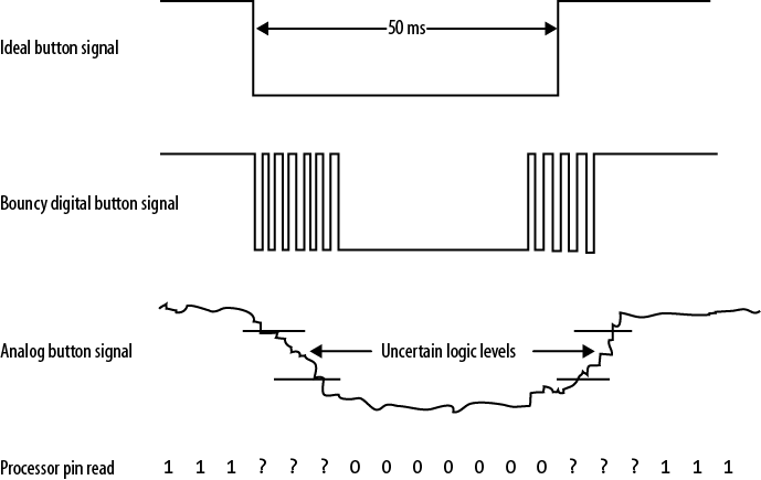
Figure 4-6 shows an analog view of what could happen when a button is pressed and only slowly goes into effect. (What really happens can be a lot more complicated, depending on whether the bouncing is due primarily to a mechanical or electrical cause.) Note that there are parts of the analog signal where the signal is neither high nor low, but somewhere in between. Since your I/O line is a digital signal, it canât represent this indeterminate value and can behave badly. A digital signal full of edges would cause the code to believe multiple presses happened per user action. The result would be inconsistent and frustrating to the user. Worse, interrupting on such a signal can lead to processor instability, so letâs go back to polling the signal.
Debouncing is the technique used to eliminate the spurious edges. Although it can be done in hardware or software, weâll focus on software. See Jack Ganssleâs excellent web article on debouncing (in the section Further Reading) for hardware solutions.
Tip
Many modern switches have a very short period of uncertainty. Switches have datasheets, too; check yours to see what the manufacturer recommends. Beware that trying to empirically determine whether you need debouncing might not be enough, as different batches of switches may act differently.
You still want to look for the rising edge of the signal, where the user releases the button. To avoid the garbage near the rising and falling edges, youâll need to look for a relatively long period of consistent signal. How long that is depends on your switch and how fast you want to respond to the user.
To debounce the switch, take multiple readings (aka samples) of the pin at a periodic interval several times faster than youâd like to respond. When there have been several consecutive, consistent samples, alert the rest of the system that the button has changed.
You will need three variables:
The current raw reading of the I/O line
A counter to determine how long the raw reading has been consistent
The debounced button value used by the rest of the code
How long debouncing takes (and how long your system takes to respond to a user) depends on how high the counter needs to increment before the debounced button variable is changed to the current raw state. The counter should be set so that the debouncing occurs over a reasonable time for that switch.
If there isnât a specification for it in your product, consider how fast buttons are pressed on a keyboard. If advanced typists can type 120 words per minute, assuming an average of five characters per word, they are hitting keys (buttons) about 10 times per second. Figuring that a button is down half the time, you need to look for the button to be down for about 50 ms. (If you really are making a keyboard, you probably need a tighter tolerance because there are faster typists.)
For our system, the mythical switch has an imaginary datasheet stating that the switch will ring for no more than 12.5 ms when pressed or released. If the goal is to respond to a button held down for 50 ms or more, we can sample at 10 ms (100 Hz) and look for five consecutive samples.
Using five consecutive samples is pretty conservative. You may want to adjust how often you poll the pinâs level so you need only three consecutive samples to indicate that the button state has changed.
Tip
Strike a balance in your debouncing methodology: consider the cost of being wrong (annoyance or catastrophe?) and the cost of doing it better (developer time and processor cycles).
In the previous falling-edge interrupt method of handling the button press, the state of the button wasnât as interesting as the change in state. To that end, weâll add a fourth variable to simplify the main loop.
read button:
  if raw reading same as debounced button value,
    reset the counter
  else
    decrement the counter
    if the counter is zero,
      set debounced button value to raw reading
      set changed to true
      reset the counter

main loop:
  if time to read button,
    read button
    if button changed and button is no longer pressed
      set button changed to false
      set the delay period (reset or halve it)
  if time to toggle the LED,
    toggle LED
  repeat
Note that this is the basic form of the code. There are many options that can depend on your systemâs requirements. For example, do you want it to react quickly to a button press but slowly to a release? There is no reason the debounce counter needs to be symmetric.
In the preceding pseudocode, the main loop polls the button again instead of using interrupts. However, many processors have timers that can be configured to interrupt. Reading the button could be done in a timer to simplify the main function. The LED toggling could also happen in a timer. More on timers soon, but first, marketing has another request.
Marketing has a number of LEDs to try out. The LEDs are attached to different pins. Use the button to cycle through the possibilities.
Weâve handled the button press, but the LED subsystem knows only about the output on pin 1_2 on the v1 board or 1_3 on the v2 board. Once youâve initialized all the LEDs as outputs, you could put a conditional (or switch) statement in your main loop:
If number button presses = 0, toggle blue LED
If number button presses = 1, toggle red LED
If number button presses = 2, toggle green LED
To implement this, youâll need to have three different LED subsystems or (more likely) your LED toggle function will need to take a parameter. The former represents a lot of copied code (almost always a bad thing), whereas the latter means the LED function will need to map the color to the I/O pin each time it toggles the LED (which consumes processor cycles).
Our goal here is to create a method to use one particular option from a list of several possible objects. Instead of making the selection each time (in the main loop or in the LED function), you can select the desired LED when the button is pressed. Then the LED toggle function is agnostic about which LED it is changing:
main loop:
  if time to read button,
    read button
    if button changed and button is no longer pressed
      set button changed to false
      change which LED

  if time to toggle the LED,
    toggle LED
  repeat
By adding a state variable, we use a little RAM to save a few
processor cycles. State variables tend to make a system confusing,
especially when the change which LED
section of the code is separated from toggle
LED. Unraveling the code to show how a state variable controls
the option can be tedious for someone trying to fix a bug (commenting
helps!). However, the state variable simplifies the LED toggle function
considerably, so there are times where a state variable is worth the
complications it creates.
However, we can go beyond a state variable to something even more flexible. Earlier we saw that abstracting the I/O pins from the board saves us from having to rewrite code when the board changes. We can also use abstraction to deal with dynamic changes (such as which LED is to be used). For this, weâll use a technique called dependency injection.
Before, we were hiding the I/O pin in the LED code (creating a hierarchy of functions that depend only on the lower levels). With dependency injection, weâll remove the dependency of LED code upon the I/O pin by passing an I/O handler as a parameter to the LED initialization code. The I/O handler will know which pin to change and how to change it, but the LED code will know only how to call the I/O handler.
An oft-used example to illustrate dependency injection relates engines to cars. The car, the final product, depends on an engine to move. The car and engine are made by the manufacturer. Though the car cannot choose which engine to install, the manufacturer can inject any of the dependency options that the car can use to get around (e.g., the 800-horsepower engine or the 20-horsepower one).
Tracing back to the LED example, the LED code is like the car and depends on the I/O pin to work, just as the car depends on the engine. However, the LED code may be made generic enough to avoid dependence on a particular I/O pin. This allows the main function (our manufacturer) to install an I/O pin appropriate to the circumstance instead of hardcoding the dependency at compile time. This technique allows you to compose the way the system works at runtime.
In C++ or other object-oriented languages, to inject the dependency, we pass a new I/O pin handler object to the LED whenever a button is pressed. The LED module would never know anything about which pin it was changing or how it was doing so. The variables to hide this are set at initialization time (but do remember that these are variables, consuming RAM and cluttering the code).
Dependency injection is a very powerful technique, particularly if your LED module were to do something a lot more complicated, for instance, output Morse code. If you passed in your I/O pin handler, you could reuse the Morse code LED output routine for any processor. Further, during testing, your I/O pin handler could print out every call that the LED module made to it instead of (or in addition to) changing the output pin.
However, the car engine example illustrates one of the major problems with dependency injection: complexity. It works fine when you only need to change the engine. But once you are injecting the wheels, the steering column, the seat covers, the transmission, the dashboard, and the body, the car module becomes quite complicated, with little intrinsic utility of its own.
The aim of dependency injection is to allow flexibility. This runs contrary to the goal of the facade pattern, which reduces complexity. In an embedded system, dependency injection will take more RAM and a few extra processor cycles. The facade pattern will almost always take more code space. You will need to consider the needs and resources of your system to find a reasonable balance.
Using the button to change the blinking speed was helpful, but marketing has found a problem in the uncertainty introduced into the blink rate. Instead of cutting the speed of the LED in half, they want to use the button to cycle through a series of precise blink rates: 6.5 times per second (Hz), 8.5 Hz, and 10 Hz.
This request seems simple, but it is the first time weâve needed to do anything with time precision. Before, the system could handle buttons and toggle the LED generally when it was convenient. Now the system needs to handle the LED in real time. How close you get to âpreciseâ depends on the parameters of your system, mainly on the accuracy and precision of your processor input clock. Weâll start by using a timer on the processor to make it more precise than it was before, and then see if marketing can accept that.
In principle, a timer is a simple counter measuring time by accumulating a number of clock ticks. The more deterministic the master clock is, the more precise the timer can be. Timers operate independently of software execution, acting in the background without slowing down the code at all.
To set the frequency of the timer, you will need to determine the clock input. This may be your processor clock (aka the system clock, or master clock), or it may be a different clock from another subsystem (for instance, many processors have a peripheral clock).
For example, the ATtiny45 has a maximum processor clock of 4 MHz. We want the LED to be able to blink at 10 Hz, but that means interrupting at 20 Hz (interrupt to turn it on, then to turn it off). This means weâll need a division of 200,000. The ATtiny45 is an 8-bit processor; it has two 8-bit timers and a 16-bit timer. Neither size of timer will work to count up that high (see the sidebar System Statistics). However, the chip designers recognized this issue and gave us another tool: the prescale register, which divides the clock so that the counter increments at a slower rate.
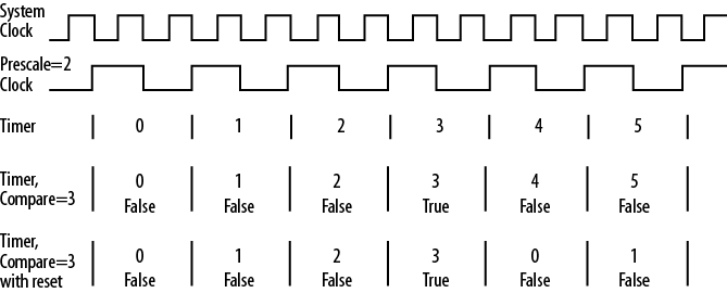
The effect of the prescale register is seen in Figure 4-7. The system clock toggles regularly. With a prescale value of two, the prescaled clock (the input to our timer subsystem) toggles at half the system clock speed. The timer counts up. The processor notes when the timer matches the compare register (set to 3 in the diagram). When the timer matches, it may either continue counting up or reset.
Before getting back to the timer on the ATtiny45, note that the registers needed to make a timer work consist of the following:
- Timer counter
This holds the changing value of the timer (the number of ticks since the timer was last reset).
- Compare (or match) register
When the timer counter equals this register, an action is taken. There may be more than one compare register for each timer.
- Action register
This register sets up an action to take when the timer and compare register are the same. (For some timers, these actions are also available when the timer overflows, which is like having a compare register set to the maximum value of the timer counter.) There are four types of possible actions to be configured:
Interrupt (or not)
Stop or continue counting
Reset the counter (or not)
Set an output pin to high, low, toggle, or nothing
- Clock configure register (optional)
This register tells a subsystem which clock source to use, though the default may be the system clock. Some processors have timers that even allow a clock to be attached to an input pin.
- Prescale register
As shown in Figure 4-7, this divides the clock so that it runs more slowly, allowing timers to happen for relatively rare events.
- Control register
This sets the timer to start counting once it has been configured. Often the control register also has a way to reset the timer.
- Interrupt register (may be multiple)
If you have timer interrupts, you will need to use the appropriate interrupt register to enable, clear, and check the status of each timer interrupt.
Setting up a timer is processor-specific, and the user manual generally will guide you through setting up each of these registers. Your processor user manual may give the registers slightly different names.
Warning
Instead of a compare register, your processor might allow you to trigger the timer actions only when the timer overflows. This is an implicit match value of two to the number of bits in the timer register minus 1 (e.g., for an 8-bit timer, (28)â1 = 255). By tweaking the prescaler, most timer values are achievable without too much error.
Timers are made to deal with physical timescales, so you need to relate them from a series of registers to an actual time. Remember that the frequency (for instance, 14 Hz) is inversely proportional to the period.
The basic equation for the relationship between the timer frequency, clock input, prescaler, and compare register is:
timerFrequency = clockIn/(prescaler * compareReg)
This is an optimization problem. You know the clockIn
and the goal, timerFrequency. You need to adjust the
prescaler and compare register until the timer frequency is close enough
to the goal. If there were no other limitations, this would be an easy
problem to solve (but it isnât always so easy).
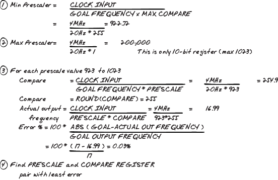
Returning to the ATtiny45âs 8-bit timer, 4 MHz system clock, and goal frequency of 20 Hz, we can export the constraints weâll need to use to solve the equation:
These are integer values, so the prescaler and compare register have to be whole numbers. This constraint is true for any processor.
The compare register has to lie between 0 and 255 (because the timer register is eight bits in size).
The prescaler on the ATtiny45 is 10 bits, so the maximum prescaler is 1023. (The size of your prescaler may be different.)
The prescaler for this subsystem is not shared with other peripherals, so we donât need to be concerned about this potential constraint for our solution.
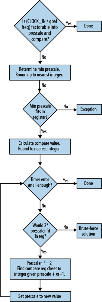
There are several heuristics for finding a prescaler and compare register that will provide the timer frequency needed (see Figure 4-8).
Note
I asked two math professors how to solve this problem in a generic manner. The answers I got back were interesting. The most interesting part was learning that this problem is NP-complete for two reasons: integers are involved, and it is a nonlinear, two-variable problem. Thanks, Professor Ross and Professor Patton!
We can determine the minimum prescaler by rearranging the equation and setting the compare register to its maximum value:
prescaler = clockIn/(compareReg*timerFrequency) minPrescaler
      = 4 MHz/(255 * 20 Hz)
Unfortunately, the resulting prescaler value is a floating-point number (784.31). If you round down (784), the timer value will be above the goal. If you round up, you may be able to decrease the compare register to get the timer value to be about right.
In this case, we end up with a timer of 19.98 Hz, which is an error of less than a tenth of a percent off. However, marketing asked for high precision, and there are some methods to find a better prescaler.
First, note that you want the product of the prescaler and compare register to equal the clock input divided by the goal frequency:
prescaler * compareReg = 4 MHz/20 Hz = 200,000
This is a nice, round number, easily factored into 1,000
(prescaler) and 200 (compare register).
This is the best and easiest solution to optimizing
prescaler and compareReg: determine the factors of
(clockIn/timerFrequency) and arrange them into
prescaler and
compareReg. However, this requires the
(clockIn/timerFreq) to be an integer and the factors to
split easily into the sizes allowed for the registers. It isnât always
possible to use this method.
We can see this as we move along to another blink frequency requested by marketing (8.5 Hz, or an interrupt frequency of 17 Hz):
prescaler * compareReg = 4 MHz/17 Hz = 235294.1
There is no simple factorization of this floating-point number. We can verify that a result is possible by calculating the minimum prescaler (we did that earlier by setting the compare register to its maximum value). The result (923) will fit in our 10-bit register. We can calculate the percent error using the following:
error = 100*(goal frequency - actual)/goal
With the minimum prescaler, we get an error of 0.03%. This is pretty close, but we may be able to get closer.
Set the prescaler to its maximum value, and see what the options are. In this case, a prescaler of 1,023 leads to a compare value of 230 and an error of less than 0.02%, a little better. But can we reduce the error further?
For larger timers, you might try a binary search for a good value, starting out with the minimum prescaler. Double it. Look at the prescaler values that are +/â 1 to find a compare register that is the closest whole number. If the resulting timer is not close enough, repeat the doubling of the modified prescaler. Unfortunately, with our example, we canât double our prescaler and stay within the bounds of the 10-bit number.
Finally, another way to find the solution is to use a script or program (e.g., Matlab or Excel) and use brute force to try out the options, as shown in Figure 4-9. Start by finding the minimum prescaler value and the maximum prescaler value (by setting the compare register to 1). Limit the minimum and maximum so they are integers and fit into the correct number of bits. Then, for each whole number in that range, calculate the compare register for the goal timer frequency. Round the compare register to the nearest whole number, and calculate the actual timer frequency. This method led to a prescaler of 997, a compare register of 236, and a tiny error of 0.0009%. A brute-force solution like this will give you the smallest error, but will probably take the most developer time. Determine what error you can live with, and go on to other things once youâve met that goal.
Brute force works well for 17 Hz, but when you get the goal output of 13 Hz, the minimum prescaler that you calculate is more than 10 bits. The timer cannot fit in the 8-bit timer. This is shown as an exception in the flowchart (Figure 4-8). The simplest solution is to use a larger timer if you can. The ATtiny45âs 16-bit timer can alleviate this problem because its maximum compare value is 65535 instead of the 8-bit 255, so we can use a smaller prescaler.
If a larger timer is unavailable, another solution is to disconnect the I/O line from the timer and call an interrupt when the timer expires. The interrupt can increment a variable and take action when the variable is large enough. For example, to get to 13 Hz, we could have a 26 Hz timer and toggle the LED every other time the interrupt is called. This method is less precise because there could be delays due to other interrupts.
Once you have determined your settings, the hard part is over, but there are a few more things to do:
Remove the code in the main function to toggle the LED. Now the main loop will need only a set of prescale and compare registers to cycle through when the button is pressed.
Configure the pin. Some processors will connect any timer to any output, whereas others will allow a timer to change a pin only with special settings. For the processor that doesnât support a timer on the pin, you will need to have an interrupt handler in the code that toggles only the pin of interest.
Configure timer settings and start the timer.
Market research has shown that potential customers are bothered by the brightness of the LED, saying its laser-like intensity is blinding them. Marketing wants to try out different brightness settings (100%, 80%, 70%, and 50%), using the button to switch between the options.
This assignment gives us a fine opportunity to explore pulse-width modulation (PWM), which determines how long a pin stays high or low. PWMs operate continuously, turning a peripheral on and then off on a regular schedule. The cycle is usually very fast, on the order of milliseconds.
PWM signals often drive motors and LEDs (though motors require a bit more hardware support). Using PWM, the processor can control the amount of power the hardware gets. Using some inexpensive electronics, the output of a PWM pin can be smoothed to be the average signal. For LEDs, though, no additional electronics are necessary. The brightness is simply relative to the amount of time the LED is on during each cycle.
A timer is a set of pulses that are all alike, so the timer signal is 50% up and 50% down (this is known as 50% duty cycle). In PWM, the pulsesâ widths change depending on the situation. So a PWM can have a different ratio. A PWM with a 100% duty cycle is always on, like a high level of an output pin. And a 0% duty cycle represents a pin that has been driven (or pulled) low. The duty cycle represents the average value of the signal, as shown by the dashed line in Figure 4-10.
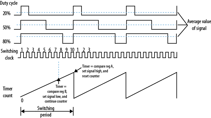
Given the timer from the previous chapter, we could implement a PWM with an interrupt. For our 20 Hz LED example, we had a compare register of 200 so that every 200 ticks, the timer would do something (toggle the LED). If we wanted the LED to be on 80% of the time with a 20 Hz timer (instead of the 50% we were doing earlier), we could ping-pong between two interrupts that would set the compare register at every pass:
Timer interrupt 1
Turn on LED.
Set the compare register to 160 (80% of 200).
Reset the timer.
Timer interrupt 2
Turn LED off.
Set the compare register to 40 (20% of 200).
Reset the timer.
With a 20 Hz timer, this would probably look like a very quick series of flashes instead of a dim LED. The problem is that the 20 Hz timer is too slow. The more you increase the frequency, the more the LED will look dim instead of blinking. However, a faster frequency means more interrupts.
There is a way to carry out this procedure in the processor. In the previous section, the configurable actions included whether to reset the counter as well as how to set the pin. Many timers have multiple compare registers and allow different actions for each compare register. Thus, a PWM output can be set with two compare registers, one to control the switching frequency and one to control the duty cycle.
For example, the bottom of Figure 4-10 shows a timer counting up and being reset. This represents the switching frequency set by a compare register. Weâll name this compare register A and set it to 100. When this value is reached, the timer is reset and the LED is turned on. The duty cycle is set with a different register (compare register B, set to 80) that turns the LED off but allows the timer to continue counting.
Which pins can act as PWM outputs depends on your processor, though often they are a subset of the pins that can act as timer outputs. The PWM section of the processor user manual may be separate from the timer section. Also, there are different PWM controller configurations, often for particular applications (motors are often finicky about which type of PWM they require).
For our LED, once the PWM is set up, the code only needs to modify the duty cycle when the button is pressed. As with timers, the main function doesnât control the LED directly at all.
Although dimming the LED is what marketing requested, there are other neat applications you can try out. To get a snoring effect, where the LED fades in and out, youâll often need to modify the duty cycle. If you have tricolor LEDs, you can use PWM control to set the three LED colors to different levels, providing a whole palette of options.
Marketing has found the perfect LED (blue), blink rate (8 Hz), and brightness (100%). They are ready to ship the product as soon as you set the parameters.
It all seems so simple to just set the parameters and ship the code. However, what does the code look like right now? Did the timer code get morphed into the PWM code, or is the timer still around? With a brightness of 100%, the PWM code isnât needed any longer. In fact, the button code can go. The ability to choose an LED at runtime is no longer needed. The old board layout can be forgotten in the future. Before shipping the code and freezing development, letâs try to reduce the spaghetti into something less tangled.
A product starts out as an idea and often takes a few iterations to solidify into reality. Engineers often have good imaginations for how things will work. Not everyone is so lucky, so a good prototype can go a long way toward defining the goal.
However, keeping around unneeded code clutters the code base (see the left side of Figure 4-11). Unused code (or worse, code that has been commented out) is frustrating for the next person who doesnât know why things were removed. Avoid that as much as possible. Instead, trust that your version control system can recover old code. Donât be afraid to release a development version internally. It will help you find the removed features after you prune the code for shipment.
In this example, many things are easy to remove because they just arenât needed. One thing that is harder to decide about is the dependency injection. It increases flexibility for future changes, which is a good reason for leaving it in. However, when you have to allocate a specific timer to a specific I/O pin, the configuration of the system becomes more processor-dependent and rigid. The cost of forcing it to be flexible can be high if you try to build a file to handle every contingency. In this case, I considered the idea and weighed the cost of making a file Iâd never want to show anyone with the benefit of reducing the chance of writing bugs in the I/O subsystem. I chose to make more readable files, even if it means a few initial bugs, but I can respect either option.
On the right side of Figure 4-11, the code base is trimmed down, using only the modules it needs. It keeps the I/O mapping header file, even with definitions for the old board because the cost is low (it is in a separated file for easy maintenance and requires no additional processor cycles). Embedded systems engineers tend to end up with the oldest hardware (karmic payback for the time at the beginning of the project when we had the newest hardware). You may need the old board header file for future development. Pretty much everything else that isnât critical can go into version control and then be removed from the project.
It hurts to see effort thrown away. But you havenât! All of the other code was necessary to make the prototypes that were required to make the product. The code aided marketing, and you learned a lot while writing and testing it. The best part about developing the prototype code is that the final code can look clean because you explored the options.
You need to balance the flexibility of leaving all of the code in with the maintainability of a code base that is easy to understand. Now that youâve written it once, trust that your future self can write it again (if you have to).
âA Guide to Debouncingâ offers mechanics, real-world experimentation, other methods for implementing your debouncing code, and some excellent methods for doing it in the hardware and saving your processor cycles for something more interesting. His whole website is worth some of your time.
LPC13xx preliminary user manual (UM10375), Rev. 00.07, 31 July 2009.
MSP430 430x2xx Family Userâs Guide (slau144e.pdf), 2008.
Atmel user manual: 8-bit Microcontroller with 2/4/8K Bytes In-System Programmable Flash (ATtiny25/V, ATtiny45/V, ATtiny85/V), Rev. 2586M-AVR-07/10.
Atmel application note: AVR 130: Setup and Use the AVR Timers
Get Making Embedded Systems now with the O’Reilly learning platform.
O’Reilly members experience books, live events, courses curated by job role, and more from O’Reilly and nearly 200 top publishers.

