Chapter 8
Printed Circuit Board Fabrication
8.1 Introduction
This chapter describes how inkjet methods can be applied to the multiple fabrication steps used in the manufacture of printed circuit boards (PCBs). We outline the current state of the art in PCB manufacturing using ‘conventional’ methods such as UV photolithography and laser direct imaging (LDI) and show where inkjet can augment or in some cases replace these processes.
8.2 What Is a PCB?
A PCB,1 as illustrated in Figure 8.1, is at the heart of every electrical and electronic device; its primary function is to provide the physical connections between the various electronic components that populate the surface of the PCB and thus form a functional electronic product.
Figure 8.1 Example of a multilayer PCB.
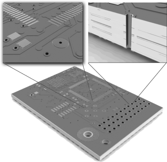
Although the PCB is commonly thought of as a straightforward, passive component, PCBs have become a key electronic component in their own right providing not only passive point-to-point connections but also designed in-board electronic characteristics such as controlled impedance, inductance, capacitance and resistance. In addition to providing the electronic interconnections, the PCB substrate also provides a mechanical platform and thermal connection to the electronic devices.
The first rigid PCB was produced in the United Kingdom shortly after World War II by ...
Get Inkjet Technology for Digital Fabrication now with the O’Reilly learning platform.
O’Reilly members experience books, live events, courses curated by job role, and more from O’Reilly and nearly 200 top publishers.

