Chapter 6Device Processing of Silicon Carbide
After epitaxial growth of SiC several processing steps are performed to fabricate electronic devices. Such processing steps include doping by ion implantation, etching, oxidation, and metallization. Figure 6.1 shows a schematic of a trench-type vertical metal-oxide-semiconductor field-effect transistor (MOSFET). The contribution of each individual process to the complete structure can be seen. The process flow in SiC device fabrication is similar to that in Si technology, but several unique technologies, with particular requirements, are also needed because of the unique physical and chemical properties of SiC.
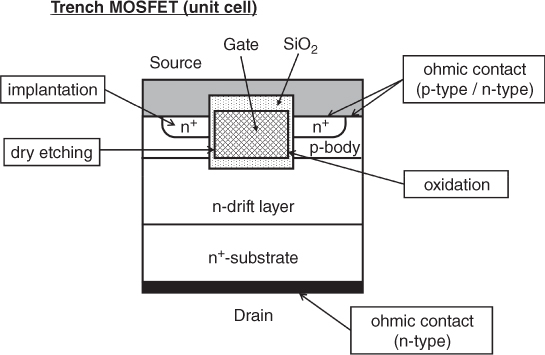
Figure 6.1 Schematic of a trench-type vertical metal-oxide-semiconductor field-effect transistor. Examples of device processing required to fabricate this device are shown.
6.1 Ion Implantation
Ion implantation is a key process in fabrication of almost all kinds of SiC devices. Wide-range doping control of both n- and p-type conductivity can be achieved by ion implantation. The major differences between ion implantation technologies for SiC and for Si are summarized as follows:
- Because of the extremely low diffusion constants of dopants within SiC, selective doping by a diffusion process is not realistic. Diffusion of most implanted impurities during post-implantation annealing is negligibly small.
- If the as-implanted ...
Get Fundamentals of Silicon Carbide Technology: Growth, Characterization, Devices and Applications now with the O’Reilly learning platform.
O’Reilly members experience books, live events, courses curated by job role, and more from O’Reilly and nearly 200 top publishers.

