Chapter 8PIC18F Hardware and Interfacing Using C: Part 1
In this chapter, we describe the first part of hardware aspects of the PIC18F4321. Topics include PIC18F4321 pins and signals, clock and reset circuits, programmed and interrupt I/O.
8.1 PIC18F Pins and Signals
The PIC18F4321 is contained in three types of packaging as follows:
- 40-pin plastic dual in-line package (PDIP)
- 44-pin quad flat no-lead plastic package (QFN)
- 44-pin thin plastic quad flat pack package (TQFP)
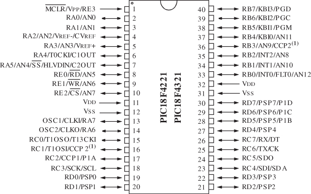
Figure 8.1 PIC18F4321 pins and signals.
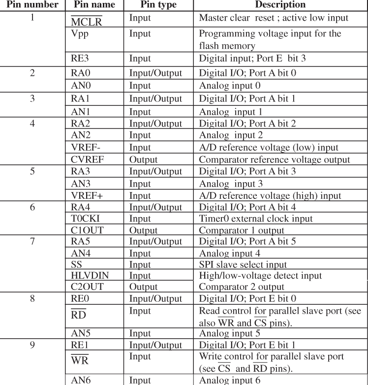
Figure 8.1 shows the PIC18F4321 pin diagram for a PDIP. A brief description of all pins and signals for the PIC18F4321 contained in the 40-pin PDIP is provided in Table 8.1. There are two VDD (Vcc) pins and two VSS (ground) pins which are not shared (multiplexed) with other pins. The range of voltages for the VDD pins are from + 4.2 V to +5.5 V. However, the VDD pins are normally connected to +5 V. The VSS pins are connected to ground. The maximum power dissipation for the PIC18F4321 is one watt. Note that multiple pins for power and ground are used in order to distribute the power and reduce noise problems at high frequencies.
Table 8.1 PIC18F4321 pinout description
 |
All other 36 pins are multiplexed (shared) with other signals. There are 36 pins ...
Get Fundamentals of Digital Logic and Microcontrollers, 6th Edition now with the O’Reilly learning platform.
O’Reilly members experience books, live events, courses curated by job role, and more from O’Reilly and nearly 200 top publishers.

