18NEMS Switch Technology
Louis Hutin and Tsu-Jae King Liu
Department of Electrical Engineering and Computer Sciences, University of California, USA
18.1 Electromechanical Switches for Digital Logic
18.1.1 Addressing the CMOS Power Crisis
For about four decades, increasing transistor density (thereby increasing chip functionality and lowering cost per function) has been carried out following a set of relatively simple transistor scaling rules [1–3]. These “constant field” device scaling guidelines were purposefully designed so that active power consumption would scale with area, hence keeping the power density constant. However, scaling the supply voltage VDD with no penalty in terms of circuit speed requires the ability to maintain a sufficient gate overdrive (VDD–VT, defining the on-state resistance of a transistor). Unfortunately, there is a fundamental limit on how much the threshold voltage VT can be reduced without causing an exponential increase in leakage current, and therefore passive power density. This limit is a direct consequence of a MOSFETs subthreshold current–voltage relationship (Figure 18.1).
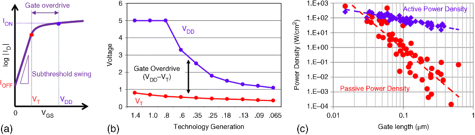
Figure 18.1 (a) Schematic typical ID-VGS of an nMOSFET. The un-scalable subthreshold swing makes IOFF increase exponentially for a linear VT shift towards 0 V. With VT fixed, a reduction of VDD provokes a decrease in ION. (b) VDD and VT scaling down to the 65 nm CMOS ...
Get Emerging Nanoelectronic Devices now with the O’Reilly learning platform.
O’Reilly members experience books, live events, courses curated by job role, and more from O’Reilly and nearly 200 top publishers.

