Self-Test
The following questions test your understanding of the concepts presented in this chapter. Use a separate sheet of paper for your drawings or calculations. Compare your answers with the answers provided following the test.
1. Draw the symbols for an NPN and a PNP bipolar transistor. Label the terminals of each.
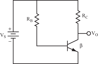
2. Draw the paths taken by the base and collector currents, as shown in Figure 3.30.
3. What causes the collector current to flow? _____
4. What is meant by the term current gain? What symbol is used for this? What is its algebraic formula? _____
Use the circuit in Figure 3.30 to answer questions 5 through 10.
5. Assume that the transistor is made of silicon. Set RB = 27 kΩ and VS = 3 volts. Find IB. _____
6. If RB = 220 kΩ and VS = 10 volts. Find IB. _____
7. Find VO when RB = 100 kΩ, VS = 10 volts, RC = 1 kΩ, and β = 50. _____
8. Find VO when RB = 200 kΩ, VS = 10 volts, RC = 1 kΩ, and β = 50. _____
9. Now use these values to find VO: RB = 47 kΩ, VS = 10 volts, RC = 500 ohms, and β = 65. _____
10. Use these values to find VO: RB = 68 kΩ, VS = 10 volts, RC = 820 ohms, and β = 75. _____
11. Draw the symbols for the two types of JFETs and identify the terminals. _____
12. What controls the flow of current in both a JFET and a BJT? _____
13. In the JFET common source circuit shown in Figure 3.31, add the correct polarities of the power supplies, ...
Get Complete Electronics Self-Teaching Guide with Projects now with the O’Reilly learning platform.
O’Reilly members experience books, live events, courses curated by job role, and more from O’Reilly and nearly 200 top publishers.

